Sample circuit layout with ltoi300 PDK#
Here we provide an example of PIC layout with the ltoi300 PDK. We start by choosing a die floorplan compatible with a submission for an LXT MPW run, then place some edge couplers for I/O at the right locations on the chip frame. We create a circuit cell with an evanescently-coupled ring resonator and connect it with the input and output edge couplers. We also create travelling wave modulators and route them optically to I/O edge couplers and electrically to wirebond pads.
from functools import partial
from pathlib import Path

import gdsfactory as gf
import numpy as np
from gdsfactory.routing import route_bundle

import ltoi300  # noqa: F401  – activates the PDK
from ltoi300.tech import LAYER
Choose the chip format and display the outline#
@gf.cell
def chip_frame():
    c = gf.get_component("chip_frame", size=(10_000, 5000), center=(0, 0))
    return c

chip_layout = chip_frame()
chip_layout

Get the O-band ring resonator and edge couplers#
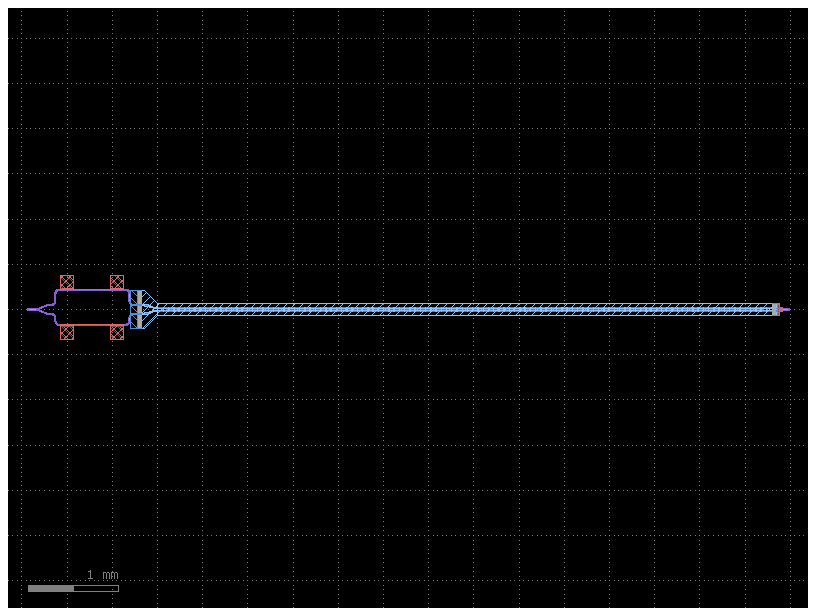
ring_resonator_oband = gf.get_component("ring_resonator_single_mode_point_coupler_oband")
ring_resonator_oband
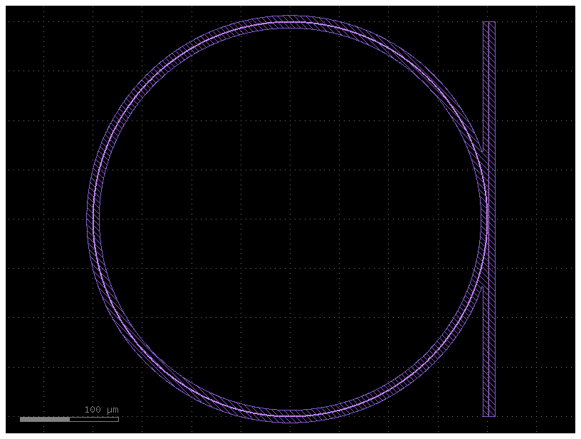
Note that we place the edge couplers such that the input port is slightly sticking outside of the chip footprint on the CHIP_EXCLUSION_ZONE layer. This is the correct placement for die singulation.
x_in = chip_layout.dxmin + 100.0
in_loc = np.array([x_in, chip_layout.dymax])
out_loc = np.array(
    [x_in + 2.5 * ring_resonator_oband.settings["ring_radius"], chip_layout.dymin]
)

ec_in = gf.Component()
ec_oband = gf.get_component("edge_coupler_oband")
ec_ref = ec_in << ec_oband
ec_ref.drotate(-90.0)
ec_ref.dmove(
    ec_ref.ports["o1"].dcenter, in_loc + [0.0, 0.5 * ec_oband.settings["input_ext"]]
)
ec_in.add_ports(ec_ref.ports)

ec_out = gf.Component()
ec_ref = ec_out << ec_oband
ec_ref.drotate(90.0)
ec_ref.dmove(
    ec_ref.ports["o1"].dcenter, out_loc - [0.0, 0.5 * ec_oband.settings["input_ext"]]
)
ec_out.add_ports(ec_ref.ports)

ecs_oband = {
    "in": ec_in,
    "out": ec_out,
}
Get the C-band ring resonator and edge couplers#
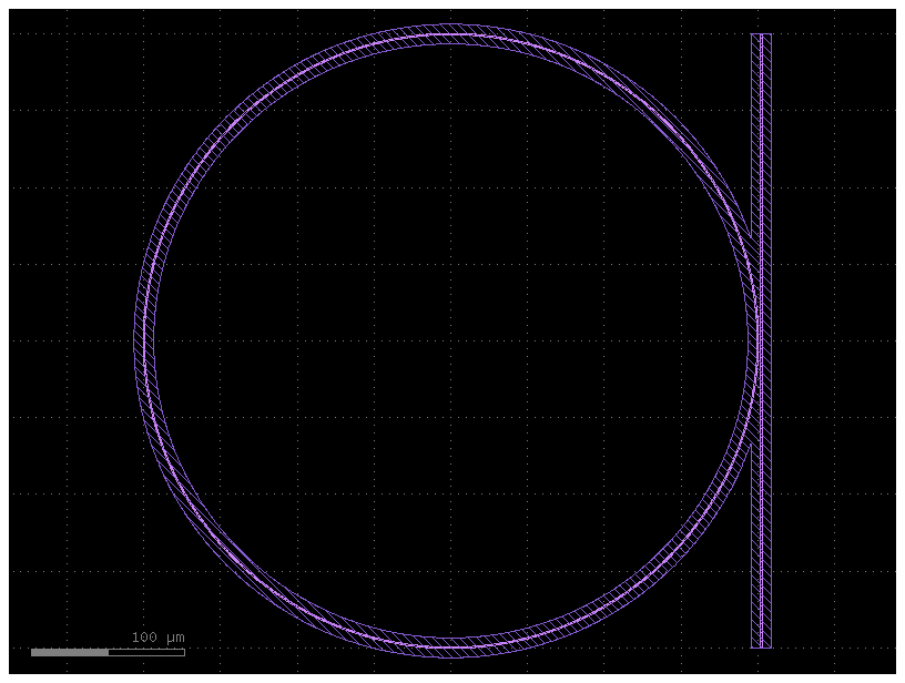
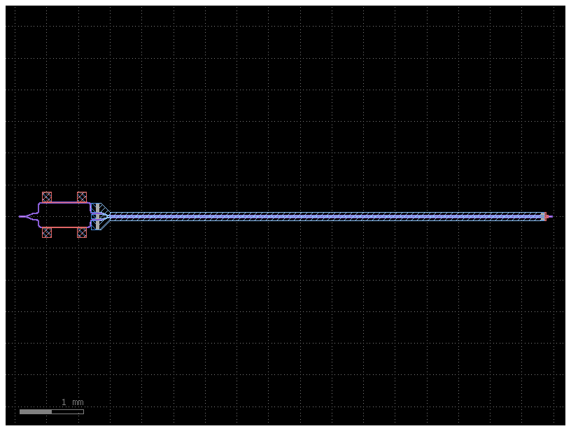
ring_resonator_cband = gf.get_component("ring_resonator_single_mode_point_coupler_cband")
ring_resonator_cband
x_in = chip_layout.dxmin + 200.0  # 100 um pitch from O-band ring EC (dxmin + 100)
in_loc = np.array([x_in, chip_layout.dymax])
out_loc = np.array(
    [x_in + 2.5 * ring_resonator_oband.settings["ring_radius"], chip_layout.dymin]
)

ec_in = gf.Component()
ec_cband = gf.get_component("edge_coupler_cband")
ec_ref = ec_in << ec_cband
ec_ref.drotate(-90.0)
ec_ref.dmove(
    ec_ref.ports["o1"].dcenter, in_loc + [0.0, 0.5 * ec_cband.settings["input_ext"]]
)
ec_in.add_ports(ec_ref.ports)

ec_out = gf.Component()
ec_ref = ec_out << ec_cband
ec_ref.drotate(90.0)
ec_ref.dmove(
    ec_ref.ports["o1"].dcenter, out_loc - [0.0, 0.5 * ec_cband.settings["input_ext"]]
)
ec_out.add_ports(ec_ref.ports)

ecs_cband = {
    "in": ec_in,
    "out": ec_out,
}
routing_roc = 60.0


@gf.cell
def ring_pass_circuit(
    communication_band="oband",
) -> gf.Component:
    if communication_band == "oband":
        ecs = ecs_oband
        coupled_ring = ring_resonator_oband
    elif communication_band == "cband":
        ecs = ecs_cband
        coupled_ring = ring_resonator_cband
    else:
        raise ValueError("communication_band must be either 'oband' or 'cband'")

    c = gf.Component()
    ring_ref = c << coupled_ring
    ring_ref.dmovex(
        -ring_ref.ports["o1"].dcenter[0] + ecs["out"].ports["o1"].dcenter[0]
    )
    if communication_band == "cband":
        ring_ref.dmovey(550.0)  # shift C-band ring 550 um higher

    # Bend spec

    routing_bend = partial(
        gf.components.bend_euler,
        radius=routing_roc,
        with_arc_floorplan=True,
    )

    # Routing to I/O

    [c << ec for ec in ecs.values()]

    route_bundle(
        c,
        ports1=[ring_ref.ports["o2"]],
        ports2=[ecs["in"].ports["o2"]],
        start_straight_length=5.0,
        end_straight_length=5.0,
        cross_section="xs_rwg700" if communication_band == "oband" else "xs_rwg900",
        bend=routing_bend,
        radius=routing_roc,
        straight="straight_rwg700_oband"
        if communication_band == "oband"
        else "straight_rwg900_cband",
    )
    route_bundle(
        c,
        ports1=[ring_ref.ports["o1"]],
        ports2=[ecs["out"].ports["o2"]],
        start_straight_length=5.0,
        end_straight_length=5.0,
        cross_section="xs_rwg700" if communication_band == "oband" else "xs_rwg900",
        bend=routing_bend,
        radius=routing_roc,
        straight="straight_rwg700_oband"
        if communication_band == "oband"
        else "straight_rwg900_cband",
    )
    text_ref = c << gf.components.text(
        f"{communication_band}" + "_ring", layer=LAYER.LABELS, size=13
    )
    text_ref.dmove(
        (
            ring_ref.dxmin + coupled_ring.settings["ring_radius"],
            (ring_ref.dymin + ring_ref.dymax) / 2,
        )
    )

    c.flatten()
    c.add_port(name="o1", port=ecs["in"].ports["o1"])
    c.add_port(name="o2", port=ecs["out"].ports["o1"])

    return c
Assemble the O-band circuit#
circuit_oband = ring_pass_circuit(communication_band="oband")
circuit_oband
Assemble the C-band circuit#
circuit_cband = ring_pass_circuit(communication_band="cband")
circuit_cband
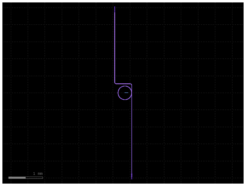
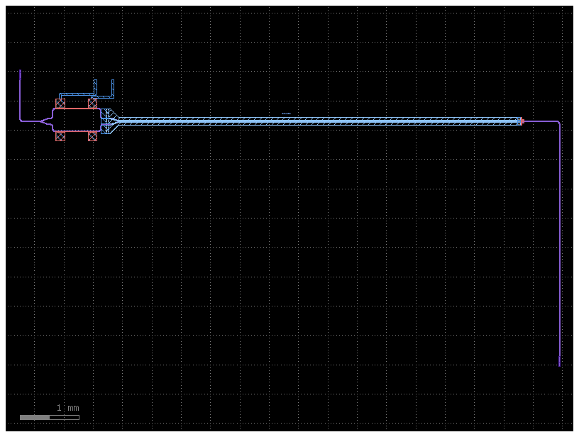
Get the O-band terminated EO modulator and edge couplers#
modulator_oband = gf.get_component(
    "terminated_mzm_1x2mmi_oband", modulation_length=6800.0, length_imbalance=120.0
)
modulator_oband
x_in = chip_layout.dxmin + 800.0
x_out = chip_layout.dxmax - 100.0
in_loc = np.array([x_in, chip_layout.dymax])
out_loc = np.array([x_out, chip_layout.dymin])

ec_in = gf.Component()
ec_oband = gf.get_component("edge_coupler_oband")
ec_ref = ec_in << ec_oband
ec_ref.drotate(-90.0)
ec_ref.dmove(
    ec_ref.ports["o1"].dcenter, in_loc + [0.0, 0.5 * ec_oband.settings["input_ext"]]
)
ec_in.add_ports(ec_ref.ports)

ec_out = gf.Component()
ec_ref = ec_out << ec_oband
ec_ref.drotate(90.0)
ec_ref.dmove(
    ec_ref.ports["o1"].dcenter, out_loc - [0.0, 0.5 * ec_oband.settings["input_ext"]]
)
ec_out.add_ports(ec_ref.ports)

ecs_oband_modulator = {
    "in": ec_in,
    "out": ec_out,
}
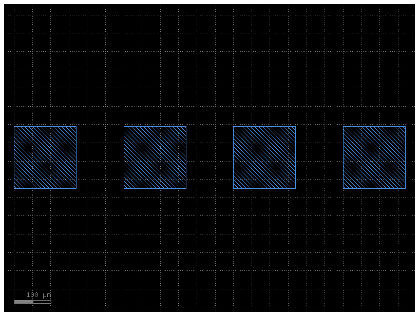
Wirebonding pads#
We add some metal pads close to the top edge of the chip. We then guide some electrical routing traces in the top metal layer to connect with the thermo-optical shifters of the modulators. This will facilitate electrical packaging and driving the heaters from an external circuit board.
@gf.cell
def bondpad_array(
    pad_size: tuple = (170, 170),
    pitch: float = 300,
    N: int = 4,
    chip_frame: gf.Component = chip_layout,
    dx: float = 1400.0,
    dy: float = 4800.0,
):
    c = gf.Component()

    pad = gf.components.pad(
        size=pad_size,
        layer=LAYER.M2,
    )
    bp = c << gf.components.pad_array(
        pad=pad,
        columns=N,
        column_pitch=pitch,
        layer=LAYER.M2,
        auto_rename_ports=True,
        centered_ports=True,
        port_orientation=-90.0,
    )

    bp.dmove(
        origin=(bp.dxmin, bp.dymin),
        destination=(chip_frame.dxmin + dx, chip_frame.dymin + dy),
    )


    c.add_ports(bp.ports)

    return c


bp_array = bondpad_array()
bp_array
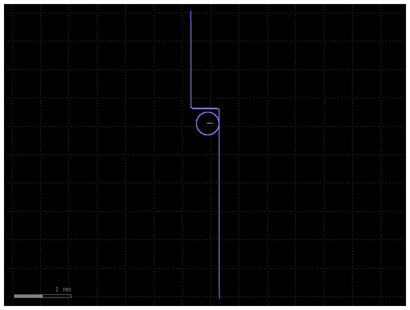
Get the C-band terminated EO modulator and edge couplers#
modulator_cband = gf.get_component(
    "terminated_mzm_1x2mmi_cband", modulation_length=6800.0, length_imbalance=120.0
)
modulator_cband
/opt/hostedtoolcache/Python/3.12.13/x64/lib/python3.12/site-packages/kfactory/decorators.py:406: UserWarning: via_array: 'signal' conductor cannot fit via rows (num_rows=0); using single solid opening.
  cell = f(**params)  # type: ignore[call-arg]
x_in = chip_layout.dxmin + 750.0
x_out = chip_layout.dxmax - 200.0
in_loc = np.array([x_in, chip_layout.dymax])
out_loc = np.array([x_out, chip_layout.dymin])

ec_in = gf.Component()
ec_cband = gf.get_component("edge_coupler_cband")
ec_ref = ec_in << ec_cband
ec_ref.drotate(-90.0)
ec_ref.dmove(
    ec_ref.ports["o1"].dcenter, in_loc + [0.0, 0.5 * ec_cband.settings["input_ext"]]
)
ec_in.add_ports(ec_ref.ports)

ec_out = gf.Component()
ec_ref = ec_out << ec_cband
ec_ref.drotate(90.0)
ec_ref.dmove(
    ec_ref.ports["o1"].dcenter, out_loc - [0.0, 0.5 * ec_cband.settings["input_ext"]]
)
ec_out.add_ports(ec_ref.ports)

ecs_cband_modulator = {
    "in": ec_in,
    "out": ec_out,
}
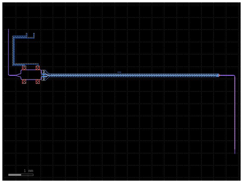
Assembly of the modulator#
routing_roc = 60.0

@gf.cell
def modulator_circuit(
    communication_band="oband",
    modulator_x_pos=-4000.0,
    modulator_y_pos=2000.0,
    bp_port_names: tuple = ("e3", "e4"),  # hashable port name strings
    waypoints_heater_routing: list = None,
) -> gf.Component:
    if communication_band == "oband":
        ecs = ecs_oband_modulator
        modulator = modulator_oband
    elif communication_band == "cband":
        ecs = ecs_cband_modulator
        modulator = modulator_cband
    else:
        raise ValueError("communication_band must be either 'oband' or 'cband'")

    c = gf.Component()
    mod_ref = c << modulator
    mod_ref.dmove(mod_ref.ports["o1"].dcenter, [modulator_x_pos, modulator_y_pos])
    # Bend spec

    routing_bend = partial(
        gf.components.bend_euler,
        radius=routing_roc,
        with_arc_floorplan=True,
    )

    # Routing to I/O

    [c << ec for ec in ecs.values()]

    route_bundle(
        c,
        ports1=[mod_ref.ports["o1"]],
        ports2=[ecs["in"].ports["o2"]],
        start_straight_length=5.0,
        end_straight_length=5.0,
        cross_section="xs_rwg700" if communication_band == "oband" else "xs_rwg900",
        bend=routing_bend,
        radius=routing_roc,
        straight="straight_rwg700_oband"
        if communication_band == "oband"
        else "straight_rwg900_cband",
    )

    route_bundle(
        c,
        ports1=[mod_ref.ports["o2"]],
        ports2=[ecs["out"].ports["o2"]],
        start_straight_length=5.0,
        end_straight_length=5.0,
        cross_section="xs_rwg700" if communication_band == "oband" else "xs_rwg900",
        bend=routing_bend,
        radius=routing_roc,
        straight="straight_rwg700_oband"
        if communication_band == "oband"
        else "straight_rwg900_cband",
    )

    # Routing to bondpad
    heater_routing_width = 40.0
    route_bundle(
        c,
        ports1=[mod_ref.ports["e3"], mod_ref.ports["e4"]],
        ports2=[bp_array.ports[bp_port_names[0]], bp_array.ports[bp_port_names[1]]],
        bend=gf.components.bend_circular,
        straight=gf.components.straight,
        auto_taper=False,
        allow_width_mismatch=True,
        layer=LAYER.M2,
        route_width=heater_routing_width,
        waypoints=waypoints_heater_routing,
        separation=10.0,
    )


    text_ref = c << gf.components.text(
        f"{communication_band}" + "_modulator", layer=LAYER.LABELS, size=13
    )
    text_ref.dmove(
        ((mod_ref.dxmin + mod_ref.dxmax) / 2, (mod_ref.dymin + mod_ref.dymax) / 2 + 100)
    )

    c.flatten()
    c.add_port(name="o1", port=ecs["in"].ports["o1"])
    c.add_port(name="o2", port=ecs["out"].ports["o1"])
    c.add_port(name="ht1", port=bp_array.ports[bp_port_names[0]])
    c.add_port(name="ht2", port=bp_array.ports[bp_port_names[1]])

    return c
modulator_circuit_oband = modulator_circuit(
    "oband", modulator_x_pos=-4000.0, modulator_y_pos=1650.0, bp_port_names=("e2", "e1")
)
modulator_circuit_oband
modulator_circuit_cband = modulator_circuit(
    "cband", modulator_x_pos=-4100.0, modulator_y_pos=650.0, bp_port_names=("e4", "e3"), waypoints_heater_routing=[(-4100, 1400), (-4100, 2200), (-3600, 2200)]
)
modulator_circuit_cband
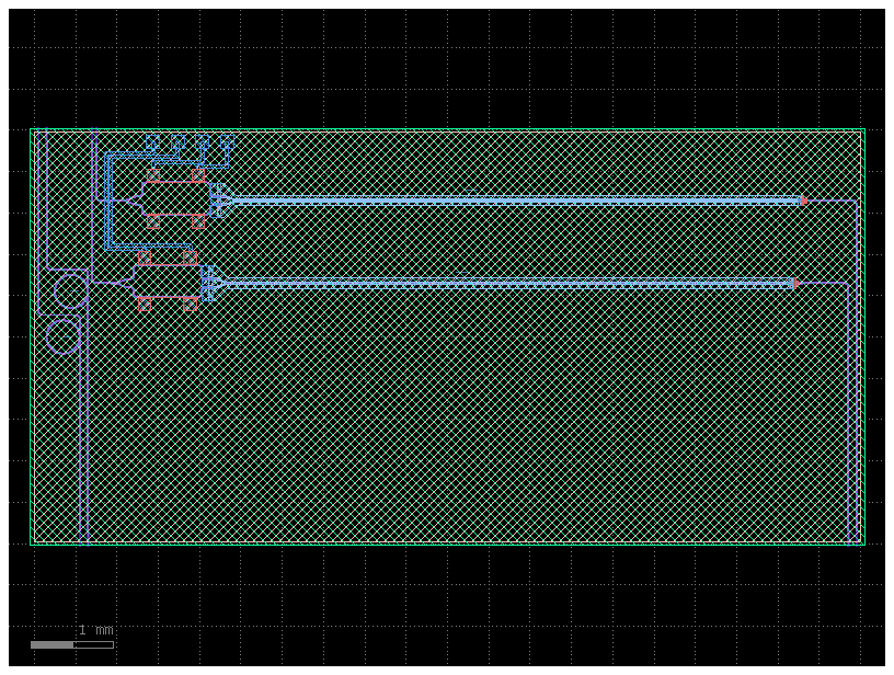
Assemble on the die outline
@gf.cell
def die_assembled(
    chip_layout=chip_layout,
) -> gf.Component:
    c = gf.Component()
    c << chip_layout
    c << circuit_oband
    c << circuit_cband
    c << modulator_circuit_oband
    c << modulator_circuit_cband
    c << bp_array

    c.add_ports(circuit_oband.ports, prefix="oband_ring_")
    c.add_ports(circuit_cband.ports, prefix="cband_ring_")
    c.add_ports(modulator_circuit_oband.ports, prefix="oband_modulator_")
    c.add_ports(modulator_circuit_cband.ports, prefix="cband_modulator_")

    return c


die = die_assembled()
die.plot()
die.show()
_ = die.write_gds(gdsdir=Path.cwd())
Recap the port positions for testing
die.pprint_ports()
┏━━━━━━━━━━━━━━━━━━━━━┳━━━━━━━┳━━━━━━━━━━━━━┳━━━━━━━━━━━━━━━━┳━━━━━━━━━━━━━━━━━━━━┳━━━━━━━━━━━━┓
┃ name                ┃ width ┃ orientation ┃ layer          ┃ center             ┃ port_type  ┃
┡━━━━━━━━━━━━━━━━━━━━━╇━━━━━━━╇━━━━━━━━━━━━━╇━━━━━━━━━━━━━━━━╇━━━━━━━━━━━━━━━━━━━━╇━━━━━━━━━━━━┩
│ oband_ring_o1       │ 0.35  │ 90.0        │ LT_SLAB (3/10) │ (-4950.0, 2530.0)  │ optical    │
│ oband_ring_o2       │ 0.35  │ 270.0       │ LT_SLAB (3/10) │ (-4450.0, -2530.0) │ optical    │
│ cband_ring_o1       │ 0.5   │ 90.0        │ LT_SLAB (3/10) │ (-4850.0, 2530.0)  │ optical    │
│ cband_ring_o2       │ 0.5   │ 270.0       │ LT_SLAB (3/10) │ (-4350.0, -2530.0) │ optical    │
│ oband_modulator_o1  │ 0.35  │ 90.0        │ LT_SLAB (3/10) │ (-4250.0, 2530.0)  │ optical    │
│ oband_modulator_o2  │ 0.35  │ 270.0       │ LT_SLAB (3/10) │ (4950.0, -2530.0)  │ optical    │
│ oband_modulator_ht1 │ 170.0 │ 270.0       │ M2 (22/0)      │ (-2965.0, 2360.0)  │ electrical │
│ oband_modulator_ht2 │ 170.0 │ 270.0       │ M2 (22/0)      │ (-2665.0, 2360.0)  │ electrical │
│ cband_modulator_o1  │ 0.5   │ 90.0        │ LT_SLAB (3/10) │ (-4300.0, 2530.0)  │ optical    │
│ cband_modulator_o2  │ 0.5   │ 270.0       │ LT_SLAB (3/10) │ (4850.0, -2530.0)  │ optical    │
│ cband_modulator_ht1 │ 170.0 │ 270.0       │ M2 (22/0)      │ (-3565.0, 2360.0)  │ electrical │
│ cband_modulator_ht2 │ 170.0 │ 270.0       │ M2 (22/0)      │ (-3265.0, 2360.0)  │ electrical │
└─────────────────────┴───────┴─────────────┴────────────────┴────────────────────┴────────────┘
Clear the gdsfactory cache#
gf.clear_cache()