Sample circuit layout with lnoi400 PDK#
Here we provide an example of PIC layout with the lnoi400 PDK. We start by choosing a die floorplan compatible with a submission for an LXT MPW run, then place some edge couplers for I/O at the right locations on the chip frame. Finally we create a circuit cell with an evanescently-coupled ring resonator and connect it with the input and output edge couplers.
from functools import partial
from pathlib import Path
import numpy as np
import lnoi400 # noqa: F401  – activates the PDK
import gdsfactory as gf
Choose the chip format and display the outline#
@gf.cell
def chip_frame():
    c = gf.get_component("chip_frame", size=(10_000, 5000), center=(0, 0))
    return c

chip_layout = chip_frame()
chip_layout

Get the circuit building blocks#
input_ext = 10.0
double_taper = gf.get_component("double_linear_inverse_taper",
input_ext=input_ext,
)
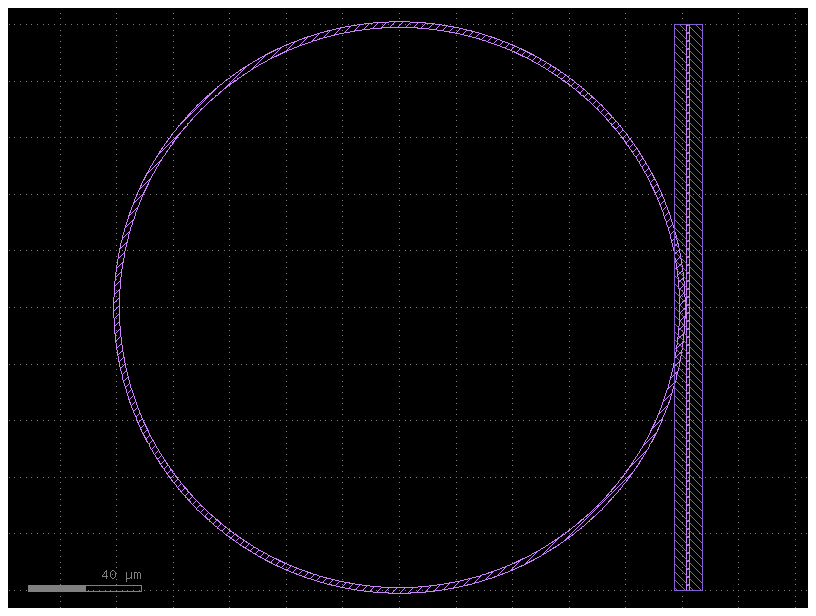
coupler_gap = 0.6
ring_radius = 100.0
ring_width = 2.0
wg_width = 1.0
ring = gf.components.ring(
layer="LN_RIDGE",
radius=ring_radius,
width=ring_width,
angle_resolution=0.15,
)
dc_wg = gf.components.straight(
length = ring_radius * 2,
cross_section="xs_rwg1000",
)
@gf.cell
def ring_with_coupler(
ring=ring,
bus=dc_wg,
gap=coupler_gap,
) -> gf.Component:
c = gf.Component()
ring_ref = c << ring
coupler_ref = c << bus
coupler_ref.drotate(90)
coupler_ref.dcenter = [
ring_ref.dxmax + gap + 0.5 * wg_width, 0.0
]
c.add_ports(coupler_ref.ports)
c.flatten()
return c
coupled_ring = ring_with_coupler()
coupled_ring
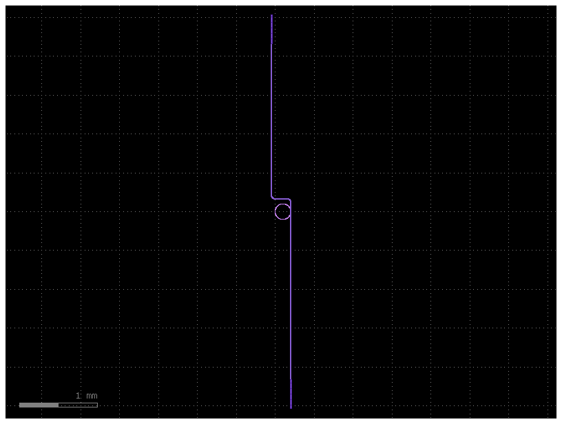
Circuit assembly#
Positioning of the I/O edge couplers. Note that we place the edge couplers such that the input port is slightly sticking outside of the chip footprint on the CHIP_EXCLUSION_ZONE layer. This is the correct placement for die singulation.
x_in = chip_layout.dxmin + 1000.0
in_loc = np.array([x_in, chip_layout.dymax])
out_loc = np.array([x_in + 2.5 * ring_radius, chip_layout.dymin])

ec_in = gf.Component()
ec_ref = ec_in << double_taper
ec_ref.drotate(-90.0)
ec_ref.dmove(
    ec_ref.ports["o1"].dcenter, in_loc + [0.0, 0.5 * input_ext]
)
ec_in.add_ports(ec_ref.ports)

ec_out = gf.Component()
ec_ref = ec_out << double_taper
ec_ref.drotate(90.0)
ec_ref.dmove(
    ec_ref.ports["o1"].dcenter, out_loc - [0.0, 0.5 * input_ext]
)
ec_out.add_ports(ec_ref.ports)

ecs = {
    "in": ec_in,
    "out": ec_out,
}
Connecting the ring with I/O
routing_roc = 75.0

@gf.cell
def ring_pass_circuit(
    coupled_ring = coupled_ring,
    ecs = ecs,
) -> gf.Component:

    c = gf.Component()
    ring_ref = c << coupled_ring
    ring_ref.dmovex(- ring_ref.ports["o1"].dcenter[0] + ecs["out"].ports["o1"].dcenter[0])

    # Bend spec

    routing_bend = partial(
        gf.components.bend_euler,
        radius=routing_roc,
        with_arc_floorplan=True,
    )

    # Routing to I/O

    [c << ec for ec in ecs.values()]

    gf.routing.route_single(
        c,
        ring_ref.ports["o2"],
        ecs["in"].ports["o2"],
        start_straight_length=5.0,
        end_straight_length=5.0,
        cross_section="xs_rwg1000",
        bend=routing_bend,
        straight="straight_rwg1000",
    )

    gf.routing.route_single(
        c,
        ring_ref.ports["o1"],
        ecs["out"].ports["o2"],
        start_straight_length=5.0,
        end_straight_length=5.0,
        cross_section="xs_rwg1000",
        bend=routing_bend,
        straight="straight_rwg1000",
    )

    c.flatten()
    c.add_port(name="o1", port=ecs["in"].ports["o1"])
    c.add_port(name="o2", port=ecs["out"].ports["o1"])

    return c

circuit = ring_pass_circuit()
circuit
/tmp/ipykernel_2657/3545328644.py:25: DeprecationWarning: route_single is less flexible and will be removed in GDSFactory10. Please use route_bundle instead.
  gf.routing.route_single(
/opt/hostedtoolcache/Python/3.12.13/x64/lib/python3.12/site-packages/gdsfactory/components/bends/bend_euler.py:112: UserWarning: {'width': 1.0} ignored for cross_section 'xs_rwg1000'
  x = gf.get_cross_section(cross_section, width=width or x.width)
/tmp/ipykernel_2657/3545328644.py:36: DeprecationWarning: route_single is less flexible and will be removed in GDSFactory10. Please use route_bundle instead.
  gf.routing.route_single(
Assemble on the die outline
@gf.cell
def die_assembled(
    chip_layout = chip_layout,
    circuit = circuit,
) -> gf.Component:
    c = gf.Component()
    c << chip_layout
    c << circuit
    c.add_ports(circuit.ports)
    return c

die = die_assembled()
die.plot()
_ = die.write_gds(gdsdir=Path.cwd())
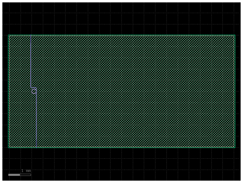
Recap the port positions for testing
die.pprint_ports()
┏━━━━━━┳━━━━━━━┳━━━━━━━━━━━━━┳━━━━━━━━━━━━━━━┳━━━━━━━━━━━━━━━━━━━━┳━━━━━━━━━━━┓
┃ name ┃ width ┃ orientation ┃ layer         ┃ center             ┃ port_type ┃
┡━━━━━━╇━━━━━━━╇━━━━━━━━━━━━━╇━━━━━━━━━━━━━━━╇━━━━━━━━━━━━━━━━━━━━╇━━━━━━━━━━━┩
│ o1   │ 0.25  │ 90.0        │ LN_SLAB (3/0) │ (-4050.0, 2530.0)  │ optical   │
│ o2   │ 0.25  │ 270.0       │ LN_SLAB (3/0) │ (-3800.0, -2530.0) │ optical   │
└──────┴───────┴─────────────┴───────────────┴────────────────────┴───────────┘
Clear the gdsfactory cache#
gf.clear_cache()